SW RF Pre-Amplifier
Description:
A radio frequency amplifier to boost SW reception. Frequency range approximately
5 to 20 MHz.

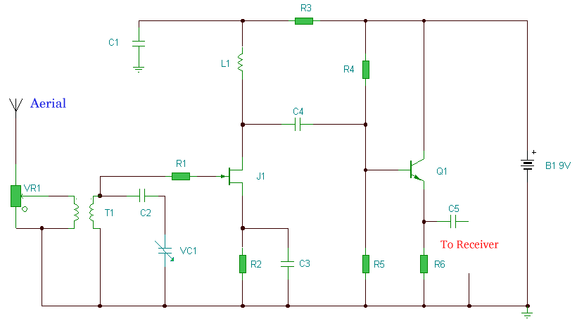
SW RF Pre-Amplifier circuit
Notes:
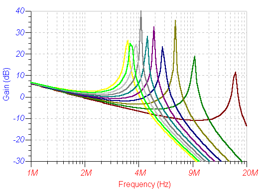
The problem with amplifying weak radio signals is that you also amplify the noise. What you can receive depends on how much background noise is present, whether it be man made interference or static. In this design the RF signal is first met by a resistive attenuator, this is necessary as strong signals could otherwise overload your receiver. The transformer T1 is would on a 1 inch diameter ferrite loop. The primary (antenna side) is 2 turns of 22 swg wire. The secondary is 4 turns of 22 swg wire. The 4 turns are spaced to occupy roughly half the coils circumference. The approximate inductance of the secondary is 20uH. To cover 5 to 20 Mhz a capacitor tuning from around 3pF to 200pF is required. A standard capacitor of 400 or 500pF (full mesh) can be used by including a series capacitor, C2 in the above Capacitors. Capacitors in series behave the same as resistors in parallel. The smallest capacitance is just less than the smallest capacitor in series and highest value also less than the highest capacitance. With a 220pF capacitor for C2 and a 500pF variable capacitor (that tunes down to 5pF) the effective capacitance tunes 143pF to about 4.8pF. This is roughly correct and not critical as the gain of the FET will amplify frequencies outside the tuned circuit range. The 2N3819 FET operates in common source. The series base resistor R1 is included to even out the response, the internal gate source impedance is thus increased by R1 at higher frequencies. The drain circuit includes a 2.5mH choke. A 4.7mH can also be used. As the Q factor of these coils are high, a series resistor R3 is introduced to flatten the response. The frequency response is shown below calculated at 10% increments of VC1:

Parts List:
R1 100k
R2 1k
R3 330
R4 47k
R5 68k
R6 4.7k
VR1 4.7k
C1 100n
C2 220p
C3 100n
C4 1n
C5 10n
VC1 500pF
L1 2.5m
J1 2N3819
Q1 BC108B
Title: SW RF Pre-Amplifier
electronic circuit
Source: unknown
Published on: 2006-01-15
Reads: 1417
Print version: ![]()
Other electronic circuits and schematics from RF circuit
-
AM FM Simultaneous Transmitter Using Digital IC
-
Micro Power AM Broadcast Transmitter
-
Sensitive Field Strength Meter
-
Simple Op-Amp Radio
-
3W FM Transmitter
-
Surveillance Transmitter Detector
-
4W FM Transmitter
-
Video to RF Modulator
-
Band 2 Preamplifier
-
AM To FM converter
