3W FM Transmitter
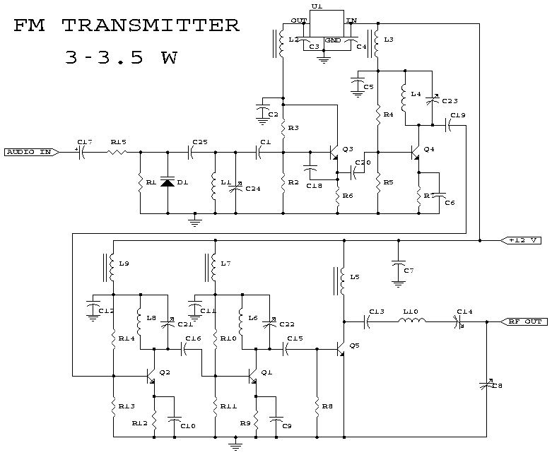
This is the schematic for an FM transmitter with 3 to 3.5 W output power that can be used between 90 and 110 MHz. Although the stability isn't so bad, a PLL can be used on this circuit.
This is a circuit that I've build a few years ago for a friend, who used it in combination with the BLY88 amplifier to obtain 20 W output power. From the notes that I made at the original schematic, it worked fine with a SWR of 1 : 1.05 (quite normal at my place with my antenna).
Schematic
Parts:
| Part | Total Qty. | Description | Substitutions |
| R1,R4,R14,R15 | 4 | 10K 1/4W Resistor | |
| R2,R3 | 2 | 22K 1/4W Resistor | |
| R5,R13 | 2 | 3.9K 1/4W Resistor | |
| R6,R11 | 2 | 680 Ohm 1/4W Resistor | |
| R7 | 1 | 150 Ohm 1/4W Resistor | |
| R8,R12 | 2 | 100 Ohm 1/4W Resistor | |
| R9 | 1 | 68 Ohm 1/4W Resistor | |
| R10 | 1 | 6.8K 1/4W Resistor | |
| C1 | 1 | 4.7pF Ceramic Disc Capacitor | |
| C2,C3,C4,C5,C7,C11,C12 | 7 | 100nF Ceramic Disc Capacitor | |
| C6,C9,C10 | 3 | 10nF Ceramic Disc Capacitor | |
| C8,C14 | 2 | 60pF Trimmer Capacitor | |
| C13 | 1 | 82pF Ceramic Disc Capacitor | |
| C15 | 1 | 27pF Ceramic Disc Capacitor | |
| C16 | 1 | 22pF Ceramic Disc Capacitor | |
| C17 | 1 | 10uF 25V Electrolytic Capacitor | |
| C18 | 1 | 33pF Ceramic Disc Capacitor | |
| C19 | 1 | 18pF Ceramic Disc Capacitor | |
| C20 | 1 | 12pF Ceramic Disc Capacitor | |
| C21,C22,C23,C24 | 4 | 40pF Trimmer Capacitor | |
| C25 | 1 | 5pF Ceramic Disc Capacitor | |
| L1 | 1 | 5 WDG, Dia 6 mm, 1 mm CuAg, Space 1 mm | |
| L2,L3,L5,L7,L9 | 5 | 6-hole Ferroxcube Wide band HF Choke (5 WDG) | |
| L4,L6,L8 | 3 | 1.5 WDG, Dia 6 mm, 1 mm CuAg, Space 1 mm | |
| L10 | 1 | 8 WDG, Dia 5 mm, 1 mm CuAg, Space 1 mm | |
| D1 | 1 | BB405 | BB102 or equal (most varicaps with C = 2-20 pF [approx.] will do) |
| Q1 | 1 | 2N3866 | |
| Q2,Q4 | 2 | 2N2219A | |
| Q3 | 1 | BF115 | |
| Q5 | 1 | 2N3553 | |
| U1 | 1 | 7810 Regulator | |
| MIC | 1 | Electret Microphone | |
| MISC | 1 | PC Board, Wire For Antenna, Heatsinks |
Notes:
1. Email Rae XL Tkacik with questions, comments, etc.
2. The circuit has been tested on a normal RF-testing breadboard (with one side copper). Make some connections between the two sides. Build the transmitter in a RF-proof casing, use good connectors and cable, make a shielding between the different stages, and be aware of all the other RF rules of building.
3. Q1 and Q5 should be cooled with a heat sink. The case-pin of Q4 should be grounded.
4. C24 is for the frequency adjustment. The other trimmers must be adjusted to maximum output power with minimum SWR and input current.
5. Local laws in some states, provinces or countries may prohibit the operation of this transmitter. Check with the local authorities.
Title: 3W FM Transmitter
electronic circuit
Source: www.aaroncake.net
Published on: 2005-02-03
Reads: 4281
Print version: ![]()
Other electronic circuits and schematics from RF circuit
-
4 Band Double Tuned Preselector
-
Coil-less FM Transmitter
-
Simple FM Transmitter
-
MK414 SW Receiver
-
Active Antenna for Medium Wave
-
ZN414 Portable AM Receiver
-
4 Transistor Transmitter
-
VHF Audio Video Transmitter
-
MK484 Portable Receiver
-
Low Distortion Crystal Oscillator