Video Clock and Message Generator
I was searching for device to generate video clock signals recently when I stumbled onto this circuit from David L. Jones of Tronnort Technology in Sydney Australia.David has a very impressive set of designs available at http://www.ozemail.com.au/~dljones/projects.htm.
This circuit allows you to superimpose a title and/or the time and sate on an incoming video signal - very useful when editing video tapes. It's also a good introduction to video signals and processing. The text that follows is from David's article:
As published in the August 1999 issue of Electronics Australia magazine.
A Low Cost Video Clock/Message Generator
by David L. Jones (dljones@ozemail.com.au)
With the proliferation of cheap CCD camera modules today it is now easier and cheaper than ever to set up your own video camera system. There are an endless number of applications such as security monitoring in a shop or other area, process monitoring in a factory or laboratory, amateur CCTV transmission, or even a fancy video doorbell to name just a few. Whilst it is all very well to be able to display and record a video signal from a camera, in many cases it is also necessary to know WHEN the image was recorded, which is essential for video security and other unattended applications. This is typically done by overlaying the time and date onto the video image itself. But how do you go about doing this ?, you can either purchase an expensive video switcher or VCR that has this facility built in, or you can build your own with the simple and low cost design to be described here!
The following design is capable of overlaying the time and date onto any existing PAL (or optionally NTSC) composite video signal. It is housed in a very neat and compact standard moulded casing and has standard 75ohm RCA video inputs and outputs. A single +9V to +15V DC supply is used to power the device, which can be taken from an existing camera supply if desired. As a bonus the design is also capable of displaying a 10 character user defined text message along with the time and date. Two on board push buttons are used to set the time/date and text message, and a 3V lithium backup battery is provided on board to maintain the time and date in the absence of power.
Circuit Overview:
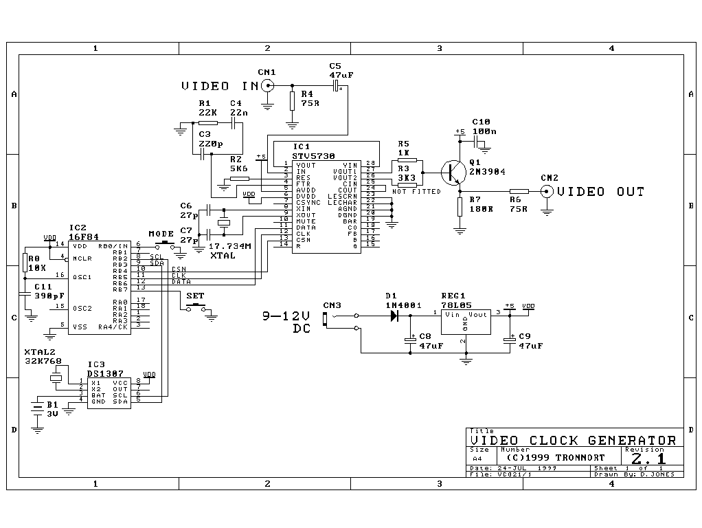
As you can see from the accompanying photos and schematic the design is extremely simple, just three IC's, a few passive components and not much else! For those who are familiar with video signals and the complexities involved in dealing with them then you may be wondering just HOW this design can do what it claims to with just three IC's!. Normally a design such as this would require sync separators, phase locked loops, horizontal and vertical timers, and that's before you even get to generating the text on the screen!. The secret of this design lies in IC1 (STV5730A), a 28 pin surface mount on-screen display generator chip manufactured by SGS-Thomson. This chip contains a complete system that takes incoming video and can overlay text anywhere onto the video signal. It contains an ASCII character generator ROM, video timing generator, vertical sync separator, PLL, voltage reference generators, video clamps, and more!. Quite a lot for one chip, but such integration is required to reduce cost in today's digital TV's and Pay TV set top boxes which this chip is designed for. IC1 has many different modes and features that are not used in this design and consequently will not be discussed here. All that IC1 requires to generate text onto a video image is a controller to tell it what needs to be displayed and where. IC2 is a microcontroller which tells IC1 what to display along with setup and configuration commands. The time and date is maintained by IC3, the DS1307, a low power clock/calendar chip manufactured by Dallas Semiconductor. This chip contains a complete 12/24 hour clock and calendar that automatically maintains the time and date in the absence of power by virtue of the 3V lithium battery. IC2 basically reads the time/date from IC3 and sends the information to IC1 to be displayed on the screen. Now lets take a look at each chip in more detail.
STV5730A Operation :
The basic internal operation of IC1 is shown in the accompanying diagram in block form. The composite video input is first terminated by R4 into 75ohms and AC coupled by C5 and then fed directly into IC1. This signal is then clamped and the composite sync signal is extracted. The input AC coupling and clamp are required in order for IC1 to able to operate off a single +5V DC supply. The sync signal controls the timing of the vertical sync generator along with the external crystal. This crystal must be 17.734MHz for PAL signals and 14.318MHz for NTSC. These timing signals are then fed into the horizontal and vertical scanning logic which drives the RAM address generator. The RAM address generator selects a character to be displayed from the internal user definable character RAM which points to a character in the character generator ROM. This ROM data then controls the luma and sync generation section (YOUT) which feeds the sync insertion and text insertion logic (via YIN). The final video signal with the text overlay emerges from the text insertion section and is buffered and passed to the video output. The video output is then fed into the emitter follower circuit of Q1 which drives the 75ohm output. Because the output is 75ohm impedance if the internal gain of IC1 was set to 0dB then the output would be 6dB down when terminated into a 75ohm load, thus the internal gain of IC1 is set to 6dB by the software in IC2 when the circuit is first powered up. The network of R1, C4 and C3 is used for the internal PLL loop.
The character brightness can be controlled via an external voltage or generated internally. In this application the brightness is controlled internally and is set to approximately 75% of the white level.
Characters can also have attributes such as blinking and a black border. These are disabled in this software however as the on screen display is designed to be as unobtrusive as possible.
IC1 requires separate analog and digital supply and ground lines and as you will see on the PCB these have been kept separate to reduce coupling of noise from the digital supply into the analog section.
Clock/Calendar Operation :
IC3 is a clock/calendar chip that maintains both time and date in BCD format. This information is read from and written to the chip via an IІC (Inter IC Control) two wire bus. The IІC bus uses two open collector TTL lines SCL (clock) and SDA (data). An IІC bus contains a master and a slave, and in this case the microcontroller IC2 is the master with IC3 being the slave. The master initiates all data transfer to and from the slave using the two control lines. Being an open collector system enables the SDA line to be used to send data both to and from the slave. IC2 has internal pull-up resistors on this these lines. IC3 stores the time and date information in BCD format in registers in the form of an internal memory map. This information is updated automatically once every second. IC2 can read this data by selecting an internal register and reading the contents out. Being in BCD format is very convenient in this application as IC2 does not have to do any decoding or calculation of the time/date information before it sends it on to IC1 to be displayed. IC3 contains a power fail detect circuit that automatically switches the internal supply over to the 3V backup battery when the supply rail gets to a low threshold. In battery backup mode the chip only requires microamps of current to keep the clock going. Thus the backup battery will last almost the shelf life of the battery. The chip also has 56 bytes of battery backed RAM that can be used for data storage, in this case the user defined text message. The chip is fully Year 2000 (Y2K) compliant with correct rollover and leap year correction.
Main Operation :
IC2 is a PIC16C558 8-bit RISC microcontroller. It has 2KB of one time programmable instruction memory, 128 bytes of RAM, 13 bidirectional I/O lines, and can operate at up to 20MHz. Many will be familiar with the popular PIC16F84 chip, the 16C558 is a pin for pin compatible chip that has more memory but without the EEPROM data storage of the 16F84. In fact the 16F84 can be used in this circuit because the code is less than 1KB and can thus fit into the 16F84. However the 16C558 is about half the cost of the 16F84. I actually used a 16F84 to develop the firmware. The discontinued 16C61 can also be used. IC2 utilises an RC oscillator formed by R8 and C11 which runs at approximately 1MHz. There is no critical timing involved in the software so an RC oscillator was a cheaper solution than a crystal. The controller uses 7 I/O lines to control everything, two for the IІC bus to IC3, three for the interface to IC1, and two for PCB mounted push buttons. When power is first applied the firmware resets and initialises various modes in IC1 and then retrieves the time, date and last text message from IC3. A main loop is then continuously executed that perform the following : 1) Read the time and date from IC3 2) Send time, date, and message information to IC3 3) Check for push button operation
The software continues in this loop indefinitely updating the display many times per second. If the MODE push button is pressed then the software will enter an edit mode that will stop updating of the on screen clock. The MODE button will move the cursor and SET button will increment the data. Pressing MODE and SET will return the software to the main loop.
REG1 is a simple +5V voltage regulator. The circuit will take less than 50mA which is well within the 100mA capability of the regulator.
Construction :
As you can see from the photo's the circuit is housed on one compact PCB measuring 88x48mm and housed directly into a compact moulded enclosure measuring 120x60x30mm. All of the external connectors, battery and push buttons are mounted on the PCB and therefore on wiring is required. The PCB mounts directly into the case on four moulded PCB mounts. Overall a very elegant solution that provides the utmost of ease in construction. Start construction of the PCB by inspecting the board for shorts and other problems, although all PCB's supplied should be solder masked so this will generally not be a problem. You should start with IC1 first, the most difficult component to mount, as it is harder to solder once all the other components are in place. Be sure to take regular anti-static precautions first. IC1 is a 28pin SO surface mount IC package mounted on the solder side of the PCB. If you haven't done any surface mount soldering before then this will be a new challenge. You will need a fine tipped temperature controlled soldering iron and 0.56mm or finer solder. You can get away with 0.71mm solder, but the finer solder produces a much better result. Soldering surface mount IC's is relatively easy if you follow a few simple rules. First of all locate pin 1 on the PCB it will be marked with a small "1", apply some solder to this pad to form a small bulge, this is to aid in holding the chip in place. Locate pin 1 on the chip then align pin 1 on the chip with the pretinned pin 1 pad on the PCB and apply the iron. The chip should sink down onto the pad and hold in place by pin 1. Ensure that the chip is centred on the other pads, if not then re-heat pin 1 and move the chip until centred. You can now solder the other pads starting with pin 15 which will hold the other corner of the chip in place. This is done like soldering a normal joint except that you will apply far less solder. Unless you are experienced, do not solder all of the pins one after the other as the chip may get overly hot and possibly get damaged. After every few pins stop and feel the chip, if it is too hot to touch then let it cool down before continuing, there is no rush. One of the major causes of surface mount component failure is excess heat, so be careful! Do one final check to ensure that there are no solder bridges between pins. Use a magnifying glass if needed.
Due to the small number of components, mounting order of the other components is not important, but it is recommended to leave the high profile components such as the RCA connectors until last. an IC socket should be used for IC2 as this chip contains firmware and thus may be updated at a later stage. Ensure the correct orientation of polarised components and don't forget the wire link near the battery. Use the component overlay as a guide. Do not solder the battery holder to the board with the battery in place and take care with the watch crystal as it can be easily damaged by excess heat.
Do not mount the PCB into the case until it has been tested.
Testing and Operation :
There is essentially no testing or setup to be done, the circuit should work first time. Insert a 3V CR2016/2032 lithium battery to the battery holder positive side up being careful not to short it on the spring loaded connector. Connect a video source to the input (camera, VCR, video generator etc) and a monitor (VCR, security monitor etc) to the output. Apply power to the board and you should immediately see a time and date display at the top of the screen. The clock may or may not be updating at this time, but this is not a problem. The time, date and text message will obviously be wrong so the first thing to do is set them correctly. This is done by pressing the MODE button to enter edit mode. The clock will stop updating on the screen and a cursor will appear under the first character. Pressing the SET button will increment the character under the cursor. The MODE button will increment the cursor by one character place. Continue moving the cursor and changing the characters until the desired information is set. Not that the time will not be updated until after you exit edit mode, so if you want the time to be very accurate then set it for a few minutes ahead of time and then wait until the correct time to exit. To exit edit mode press and hold down the MODE button and quickly press the SET button at the same time, the cursor should disappear and the time/date/message information will be written to the clock chip and the display will start updating as normal. Now disconnect and reapply power to the unit and ensure that the time/date and message show up again as expected. That is all there is to the operation of the unit, the time will be incremented once every second, and the information will be retained when the power is disconnected. All that is left now is to connect it into your desired system which will usually be just before the VCR or monitor input.
The time and date are fixed in 24hr and DD/MM/YY format respectively and the display is fixed at the top center of the screen.
A complete kit with all components including the programmed PIC chip will be available as well as individual programmed chips for those that wish to build their own customised unit. Further information is available from the authors web site at http://www.ozemail.com.au/~dljones and EMAIL on dljones@ozemail.com.au
|
Click the above for the PIC ASM Files |
Click the above for the PIC HEX Files |
Click the above for the Protel Layout Files. |
Title: Video Clock and Message Generator
electronic circuit
Source: http://www.web-ee.com
Published on: 2005-06-19
Reads: 2620
Print version: ![]()
Other electronic circuits and schematics from Video and TV
-
UHF Preamplifier
-
4 Stage 555 Timer for Video Cam Control
-
Audio / video switch
-
Composite color video signal travels on twisted-pair cable
-
S-video to composite video adapter
-
The Video / Audio Distribution Amplifier
-
Video Signal Amplifier
-
Video Line Selector
-
Driver for Multiple VGMonitors
-
Video multiplexer uses high-speed op amps