Every picture tells a story
Interestingly, digital circuits of all types (and we’ll cover a few over the next few pages) are made up using just this simple and basic configuration. Even whole computers use this basic inverter as the heart of all their complex circuits.
To make it easy and convenient to design complex digital circuits using such transistor switches, we use symbols instead of having to draw the complete transistor circuit. The symbol for an inverter is shown in Figure 10.4, and is fairly self-explanatory. The triangle represents the fact that the circuit acts as what is called a buffer — that is, connecting the input to the output of a preceding stage does not affect or dampen the preceding stage in any way. The dot on the output tells us that an inverting action has taken place, and so the output state is the opposite of the input state in terms of logic level.
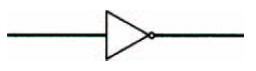
Figure 10.4 The symbol of an inverter — the simplest form of digital logic gate
To aid our understanding of digital logic circuits, input and output states are often drawn up in a table — known as a truth table, which maps the circuit’s output states as its input states change. The truth table for an inverter is shown in Figure 10.5. As you’ll see, when its input state is 1 its output state is 0. When its input is 0, its output is 1 — exactly as we’ve already hypothesised.
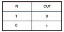
Figure 10.5 Truth table of an inverter — the circuit of Figure 10.1, and the symbol of Figure 10.4
It’s important to remember that, in both a logic symbol and in a truth table, we no longer need to know or care about voltages. All that concerns us is logic states — 0 or 1.
We can build up a simple circuit on breadboard to investigate the inverter and prove what we’ve just seen in theory. Figure 10.6 shows the circuit, while Figure 10.7 shows the circuit’s breadboard layout. The digital integrated circuit used in Figure 10.6 and Figure 10.7 is actually a collection of six inverters, all accessible via the integrated circuit’s pin connections — such an integrated circuit is commonly called a hex inverter, to signify this. We’ve simply used one of the integrated inverters in our circuit.
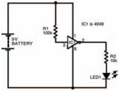
Figure 10.6 Circuit of an experiment to discover how an inverter works
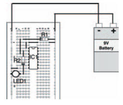
Figure 10.7 Possible breadboard layout of the circuit in Figure 10.6
The integrated circuit used is a type of integrated circuit called a CMOS device, and it’s in what’s known as the 4000 series of integrated circuits — it’s actually known as a 4049. Don’t worry about this for now, as we’ll look at more devices in the series (and another series, for that matter) later in the chapter. All you need to know for now is that it’s a standard dual-in-line (DIL) device, so you must be careful that you position it correctly in the breadboard.
Making sure that the actual integrated inverter used in our circuit has the correct input (that is, either logic 1 or logic 0) is easy. Logic 1 is effectively the same as a connection to the positive battery supply — in practice though, you should never connect an input ‘directly’ to the positive battery supply; instead always connect it using a resistor. On the other hand, logic 0 is just as effectively the same as a connection to the negative battery supply (this time though, it’s perfectly allowable to connect an input directly). In other words, when the inverter’s input is connected to positive it’s at logic 1: when connected to negative it’s at logic 0.
It’s not a good idea to leave an input unconnected (what is called ‘floating’), as it may not be at the logic level you expect it to be, so we’ve added a fairly high-valued resistor to the input of the inverter to connect it directly to the positive battery supply. This means that, under normal circumstances — that is, with no other input connected — we know that the inverter’s input is held constantly at logic 1. To connect the inverter input to logic 0, it’s a simple matter of connecting a short link between the input and the negative battery supply. This isn’t shown in the breadboard layout, but all you need to do is add it when you are ready to perform the experiment.
Measuring the output of the inverter is just as easy, and we take advantage of the fact that the output can be used to light up a light-emitting diode (LED). So, when the inverter’s output is at logic 1, the LED is lit: when the inverter’s output is at logic 0, the LED is unlit.
Once the circuit’s built, it’s a simple matter of carrying out the experiment to note the output as its input changes, and completing its truth table. Figure 10.8 is a blank truth table for you to fill in. Just note down the circuit’s output, whatever its input state is. Of course, your results should tally exactly with the truth table in Figure 10.5 — if it doesn’t, you’ve gone wrong, because as I’ve said before in this book — I can’t be wrong, can I?
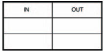
Figure 10.8 Empty truth table for your results of the experiment in Figure 10.6
<< Logically speaking