Follow me
These two op-amp formats; inverting and non-inverting amplifiers, are the basic building blocks from which most op-amp circuits are designed. They can be adapted merely by altering the values of the circuit resistances, or even by replacing the resistances with other components (such as capacitors) so that the circuits perform a vast number of possible functions.
As an example we’ll look at a couple of circuits, considering how they are designed, compared with the two basic formats. First, we’ll consider the circuit in Figure 9.9. At first sight we can see that it is a non-inverting circuit of some description — the input voltage (derived from the wiper of the preset resistor) is applied to the noninverting input of the op-amp. But in comparison with our non-inverting amplifier of Figure 9.6, there are no resistors around the amplifier; instead the output voltage is simply looped back to the inverting input. So how does it work and what does it do?
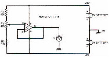
Figure 9.9 A voltage follower circuit: the output is equal to the input. This is basically a non-inverting circuit
Let’s first consider the non-inverting amplifier gain expression:

and look to see how we can apply it here. Although no resistances are in this circuit that doesn’t mean that we don’t need to consider them! Resistor R1 in the circuit of Figure 9.5 can be seen to be between pin 6 of the op-amp (the output) and pin 2 (the inverting input). In the circuit of Figure 9.9, on the other hand, there is a direct connection between pin 6 and pin 2 — in other words we can imagine that resistor R1 of this circuit is zero.
Similarly, resistor R2 of the circuit in Figure 9.5 lies between pin 2 and 0 V. Between pin 2 and 0 V of the circuit in Figure 9.9 there is no resistor — in other words we can imagine the resistance to be infinitely high.
We can put these values of resistances into the expression for gain, which gives us:

so the circuit has a gain of one i.e., whatever voltage is applied at the input is produced at the output. The circuit has a number of common names, one of which is voltage follower, which quite accurately describes its operation. Build the circuit as shown in the breadboard layout of Figure 9.10, to see for yourself that this is indeed what happens. All you need do to confirm the results is to measure the input and output voltages at a few different settings, making sure they are the same.
It may seem a bit odd that we have built a circuit, however simple, which appears to do the same job which an ordinary length of wire could perform — that is, the output voltage is the same as the input voltage. But the situation is not quite as simple as that. The circuit we have constructed, although having a gain of only one, has a very high input resistance. This means that very little current is drawn from the preceding circuit (in this case the preset resistor/voltage divider chain). On the other hand, the circuit has a very low output resistance, which means that it is capable of supplying a substantial current to any following circuits. This property gives rise to another of the circuit’s common names — resistance converter.
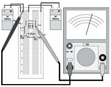
Figure 9.10 The breadboard layout of the circuit in Figure 9.9
Hint:
In practice the voltage follower is often used when the output of a circuit which is only capable of producing a small, weak current is required to be amplified. The voltage follower is used in the input stage of the amplifier to buffer the current before amplification takes place, thus preventing loading of the preceding circuit. In fact the term buffer is just another name for the voltage follower.
<< Turning things upside-down