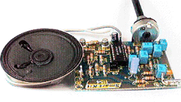
Electronic Eavesdropping Devices Detector
| The placement of electronic eavesdropping
devices in homes and companies offices is becoming - unfortunately - a usual phenomenon through the passing of the years. Espionage movies admirers, is possible to remember scenes of the placement of very small components (which had the format of a button or a lentil) in rooms or offices which are not far away from the reality. However, the detection of electronic eavesdropping devices is not so easy, even though it is known their placement. The reason is the very small format and their similarity to other things which we use every day. Using the detector that is described in this article, you can ensure the privacy of your personal life because it allows you to sweep for electronic eavesdropping devices. |
 |
|
 |
||||||||||||
| How it Works |
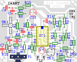
Electronic bugs are very small radio frequency transmitters, that are secretly placed in a room that is to be monitored. Since most bugs are RF sources, almost any wideband receiver can be used as a detector. Our detector detects an RF signal ranging from 1 to 1000 MHz. Figure 1 shows the schematic diagram of the detector. When the electronic bug operates, it emits an RF signal. This signal is received by the antenna (point 1 of figure 1) and is applied to the base of the transistor TR1 through a high-pass filter ( a filter that permits the passing of high frequencies). The high-pass filter consists of the capacitors C4, C5 and the resistor R7.
When low frequency signals are applied to the input of the filter, the capacitors C4 and C5 operate as open switches and the filter rejects the low frequency signals. The cut-off frequency of the high-pass filter is defined to be 60 Hz rejecting any interferences which come from the mains. The transistor TR1 is in common collector conjunction and it is used to amplify the signal. The gain that is provided is 10dB for a signal that varies in the frequency range 1 - 1000 MHz. The resistors R1, R2, R8 form the biasing network for the transistor TR1. The amplified signal is then applied, via the capacitor C6, to the anode of the diode D1. The diode is particularly manufactured to operate in high frequencies, since a common diode can not go from the conduction condition to the cut-off condition very fast preventing the appearance of reverse currents.
However the operation of the diode in the high frequencies range results in the appearance of a conduction at the beginning of the negative half period. The potentiometer P1 adjusts the proportion of the signal at the terminals of the diode D1 and applies it to the inverting input (pin 2) of the operational amplifier A1. The operational amplifier A1 is configured as a very high gain amplifier. The value of the gain is defined by the capacitor C8 and the resistors R6 and R12. With no signal input from the antenna, the output of A1 at pin 1 is near ground potential. When the antenna detects a signal in the range 1 - 1000 MHz, it applies it to the base of the transistor TR1 producing a negative-going voltage at the cathode of diode D1.
That voltage is applied to the inverting input of A1 which amplifies and inverts
the signal, producing a positive-going output at pin 1. The next stage after the
op. amp. A1 is a voltage controlled oscillator (VCO). The oscillation frequency
of VCO is controlled by the output voltage of the operational amplifier A1. The
operational amplifiers A2, A4, along with the resistors R11, R13, R14, R16, R17,
R18, R19, R20, R21, R23, the capacitor C9 and the transistor TR2 are arranged to
form a voltage-controlled oscillator (VCO) that operates out of the audio-frequency
range. As the output of A1 increases, the frequency of the VCO increases. The
VCO output, at pin 8 of the operational amplifier A4, is fed to the input of A3,
which is configured as a non-inverting unity gain (buffer) amplifier. The output
of A3 is used to drive the transistor TR3, which, in turn, drives the output
speaker

| Construction |
Before you start the construction of the circuit you must follow the basic instructions. Place and solder the socket of the IC1. Then install the passive components (resistors, capacitors) on the board checking for the right placement and orientation. After this, install the semiconductors (diode, transistors, IC). You ought to be very careful in order to avoid the overheating of the IC’s diodes and transistors terminals. Place the IC1 on its base, checking for the right orientation. Use a 25W iron solder without using soldering flux. When you have finished the structure of the circuit, check your work for the common construction errors (misoriented components, solder bridges, misplaced components), particularly where the transistors and diode are concerned.
Check if there are any dry joints. A proper joint is spread all over the pad
and is shiny. A dry one is dull, bulky and has the shape of the ball. If
everything is correct, clean the printed circuit board using a proper spray.
Finally, install the board in a metal box connecting its chassis to the ground
of the circuit (point 5). Connect the speaker to the points 2 and 3, and the
antenna to the point 1 (see figure 1). Use a 9V battery to supply the circuit.
The clip of the battery is connected to the points 4 and 5. The red wire of the
clip (positive/+) is connected to point 4, while the black one (negative/-) to
point 5.
Afterwards, stand in the middle of the room you want to check. Adjust the potentiometer in order the sound coming from the loudspeaker LS to be slightly audible. You must do this in order the external electromagnetic fields to be ignored. Begin the detection of an RF signal in the room. The loudspeaker will start to sound, when a signal in the frequency range (1 - 1000MHz) will be detected.
|
|
|
| Parts List | |
| Resistors : | Capacitors : |
| R1 = 39 KΩ | C1 = 10nF ceramic |
| R2 = 470 Ω | C2 = 4,7 μF/16V electrolytic |
| R3 = 22 Ω | C3 = 10nF ceramic |
| R4 = 100 Ω | C4 = 1nF ceramic |
| R5 = 560 Ω | C5 = 10nF ceramic |
| R6 = 1 MΩ | C6 = 10nF ceramic |
| R7 = 220 Ω | C7 = 10nF ceramic |
| R8 = 100 KΩ | C8 = 10nF ceramic |
| R9 = 4,7 KΩ | C9 = 4,7nF ceramic |
| R10 = 1,5 KΩ | C10 = 10 μF/16V electrolytic |
| R11 = 10 KΩ | Chip : |
| R12 = 220 Ω | IC1 = ΜC3403P Motorola |
| R13 = 10 KΩ | Transistors : |
| R14 = 100 KΩ | TR1 = BFR 90A |
| R15 = 470 Ω | TR2 = 2N2222 |
| R16 = 47 KΩ | TR3 = 2N2222 |
| R17 = 47 KΩ | Diode : |
| R18 = 1 KΩ | D1 = NTE 112 |
| R19 = 10 KΩ | Potesiometer : |
| R20 = 100 KΩ | P1 = 4,7K Linear ποντεσιόμετρo |
| R21 = 47 KΩ | Other : |
| R22 = 10 KΩ | ΑNT = telescopic antenna. Radio type. |
| R23 = 47 KΩ | LS = Loundspeaker 8Ω |
Title: Electronic Eavesdropping Devices Detector
electronic circuit
Source: smartkit
Published on: 2005-02-03
Reads: 1460
Print version: ![]()
Other electronic circuits and schematics from RF circuit
-
Powerful AM transmitter
-
4 Watt FM Transmitter
-
Simple FM Transmitter
-
1 Watt C-Class RF Amplifier
-
4 Band Double Tuned Preselector
-
Band 2 Preamplifier
-
TV Signal Amplifier
-
VHF Video Transmitter
-
AM Receiver
-
Low-Frequency Crystal Controlled Oscillator