Open the black box
Just as we found earlier that we could create logic gates with collections of transistors, but decided we could draw logic gates with their own symbols (rather than actually drawing all the internal transistors involved), so there are symbols for the various types of bistable — that don’t show the actual logic gates (or, indeed, the individual transistors) involved.
Figure 11.13, for example, shows the symbol for a clocked, edge-triggered, SR-type bistable, such as the circuit of Figure 11.10. It’s just a box, with the bistable’s main inputs shown on the box. Note though, that it doesn’t show whether the SR-type bistable is created from NAND gates or NOR gates (or whatever gates, or indeed whatever transistors, actually — that’s all very irrelevant!). All you need to remember is that it’s just a box showing inputs and outputs — and that it acts as a clocked, edge-triggered, SR-type bistable.

Figure 11.13 A clocked, edge-triggered, SR-type bistable symbol
Of note is the symbol used for the clock input, , which merely represents the fact that it is edge-triggered. Its function table is shown in Figure 11.14.
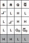
Figure 11.14 The function table of the clocked, edge-triggered, SR-type bistable of Figure 11.13
Such an approach of simplifying circuits is very common in electronics, and we’ve come across it before — the black-box approach. The approach relies on the fact that we don’t need to know how a complex circuit is constructed — we only need to know its function.
Every single one of the other logic gate types we’ve seen in this chapter can also be represented in black box block form by symbols, and to prove it, we’ll consider them all now. All you have to do is remember that if necessary they can — and sometimes are — built using logic gates, but you don’t need to know how to construct them that way because — yes, you’ve guessed it — they can be bought ready-built in IC form, in the same series (7400 and 4000) we’ve already used and are familar with.
First is the D-type bistable. Its circuit symbol is shown in Figure 11.15, while its corresponding function table is in Figure 11.16.
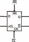
Figure 11.15 A D-type bistable symbol
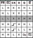
Figure 11.16 The function table of a D-type bistable, such as the one shown in Figure 11.15
Note that the inputs (preset) and (clear), are included in this D-type bistable (unlike the D-type bistable shown in Figure 11.9). These perform similar functions to the S and R inputs of the SR-type bistable. You should now be able to understand the function table. The first three rows indicate that the and inputs override all other inputs (that’s why the clock and D inputs are shown as X: because X = don’t care). Thus the outputs Q and are dependent primarily upon the logic states of the and inputs.
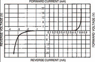
Figure 6.19 My results from the zener diode experiment are given in this graph and in Tables 6.7 and 6.8
occurs when the reverse current appears to be zero, but in fact, a small saturation current does exist — it was simply too small to measure on the meter.
Voila — a complete diode characteristic curve.
Finally, it stands to reason that any diode must have maximum ratings above which the heat generated by the voltage and current is too much for the diode to withstand. Under such circumstances the diode body may melt (if it is a glass diode such as the OA47), or, more likely, it will crack and fall apart. To make sure their diodes don’t encounter such rough treatment manufacturers supply maximum ratings which should not be exceeded. Typical maximum ratings of the two ordinary diodes we have looked at; the 1N4001 and the 0A47 are listed in Table 6.9.
There’s a couple of points to note about this JK-type bistable symbol:
- operations take place on the falling edge of the applied clock pulse;
- the last row of the function table shows a bistable operation known as toggling — in which the output state changes from whatever state it is, to the other state. This, you will of course remember — is how the T-type bistable of Figure 11.12 is created.