Other logic gates
The other logic gates we need to know about are every bit as simple as the NOT gate or the inverter. They all have a symbol, they all have a truth table, but most important, they all have a Boolean statement we can associate with them.
OR gate
The symbol of an OR gate is shown in Figure 10.10. To see how an OR gate works, however, we’ll conduct an experiment to complete a truth table. The circuit of the experiment is shown in Figure 10.11, while the breadboard layout is in Figure 10.12.
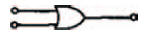
Figure 10.10 The circuit symbol for a 2-input OR gate
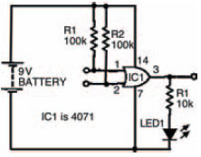
Figure 10.11 Experimental circuit to find out how an OR gate works
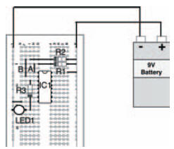
Figure 10.12 Possible breadboard layout for the experimental circuit showing OR gate operation in Figure 10.11
Build up the circuit, and fill in the blank truth table given in Figure 10.13 according to the results of the experiment as you change the circuit’s inputs. You should see that the output of the circuit is logic 1 whenever one or other of the circuit’s inputs are logic 1. Let’s say that again — whenever one ‘or’ the other — which is why it’s called an OR gate.
The results you should have got for your truth table are shown in the truth table of Figure 10.14.
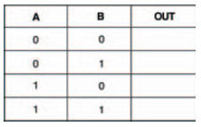
Figure 10.13 A truth table to put the results of your experiment into
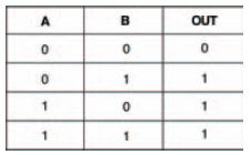
Figure 10.14 The results you should have got in your experiment
An OR gate is not quite as simple as an inverter — an inverter, after all, has only one input. An OR gate has more than one input — in theory it can have any number of inputs but, obviously, as the number of inputs increases, the resultant truth table gets more complicated.
Figure 10.15, shows a three input OR gate symbol and truth table. Being a three input gate, its truth table has eight variations. We can calculate this because, being binary digital, the circuit can have 23 = 8 variations of inputs.
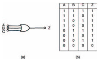
Figure 10.15 (a) the symbol for an OR gate; (b) its truth table
The truth table of the OR gate shows that output Z of the gate is 1 when either A OR B OR C is 1. In Boolean terms, this is represented by the statement:

where ‘+’ indicates the OR function and has nothing whatsoever to do with the more usual arithmetical ‘plus’ sign. Don’t be confused: just remember that every time you see the ‘+’ sign in Boolean algebra it means OR.
AND gate
As you might expect, an AND gate follows the Boolean AND statement. Figure 10.16 shows an AND gate circuit, while its breadboard layout is shown in Figure 10.17, and Figure 10.18 is a blank truth table ready for you to record the experiment’s results. As you might already expect, an AND gate is so called because its output is at logic 1 when input 1 AND input 2 are at logic 1. As a result, your experimental truth table should look like the complete truth table shown in Figure 10.19.
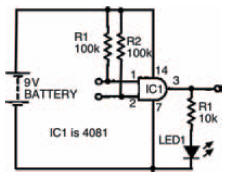
Figure 10.16 Circuit to investigate AND gate Boolean operation
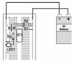
Figure 10.17 Possible breadboard layout to investigate the circuit of Figure 10.16
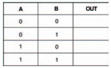
Figure 10.18 Truth table for you to record your results of your experiment
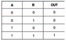
Figure 10.19 How your results should look
Translating this into a Boolean statement for a three input AND gate with inputs A, B, and C (shown as a symbol and as a truth table in Figure 10.20), we can see that its output Z is 1, only when inputs A AND B AND C are 1. The Boolean statement is therefore:

where ‘.’ indicates the Boolean AND expression.
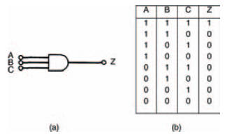
Figure 10.20 (a) a three input AND gate; (b) its truth table
NOR gate
The NOR gate’s function can be calculated from its name ‘NOR’. Effectively, we can think of this as meaning ‘NOT OR’. In other words, it’s an OR gate and a NOT gate (that is, an inverter) in series.
The circuit of our experiment to look at NOR gates is shown in Figure 10.21, while a possible breadboard layout for the circuit is given in Figure 10.22. A blank truth table for you to fill in is shown in Figure 10.23.
Figure 10.21 Circuit to find out the function of a NOR gate
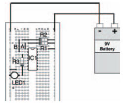
Figure 10.22 Possible breadboard layout to build the circuit of Figure 10.21
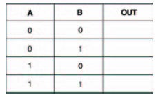
Figure 10.23 Blank truth table to complete with the results of your experiment
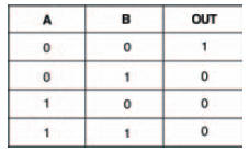
Figure 10.24 A completed truth table for the experiment in Figure 10.21
In Boolean terms, the output of a NOR gate is the exact inverse of the OR gate’s output. When applied to the three input NOR gate and its truth table shown in Figure 10.25, we can see that the NOR gate’s output is 1 when neither A NOR B NOR C is 1 — in other words, the exact inverse of the OR gate’s output.
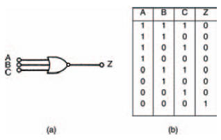
Figure 10.25 (a) a NOR gate; (b) its truth table
As a Boolean statement this is written:

NAND gate
You should be able to work out for yourself what the NAND in NAND gate stands for: NOT AND. So, if you’ve followed the last bit about NOR gates, you might also be able to work out its Boolean statement. Nevertheless, it’s best to see things for ourselves, and the circuit shown in Figure 10.26 is the experiment we need to carry out to understand what’s happening. Figure 10.27 is a possible breadboard layout for the circuit in Figure 10.26.
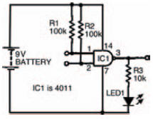
Figure 10.26 Circuit to investigate a NAND gate
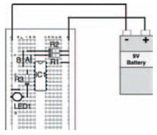
Figure 10.27 Breadboard layout to build the circuit of Figure 10.26
Meanwhile Figure 10.28 is a blank truth table for you to fill in with your results.
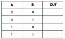
Figure 10.28 Blank truth table, ready for the results of your experiment
Figure 10.29 is the completed truth table for a NAND gate, and yours should be the same (if not, why not, eh?).
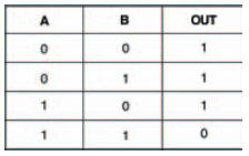
Figure 10.29 Completed truth table for a NAND gate
And, for the sake of completeness, Figure 10.30 shows a three input NAND gate and its truth table.
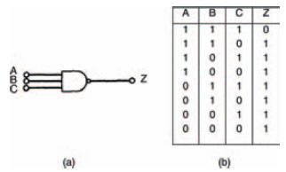
Figure 10.30 A three input NAND gate (a) symbol, (b) truth table
Actually, it’s quite difficult to express a NAND gate’s operation in words, but here goes: it’s a gate whose output Z is 1 when NOT A AND NOT B AND NOT C is 1. Err… yeah, right!
A better way is to express it as the Boolean statement:

which, no doubt you have already worked out!
Haven’t you?
<< Boolean algebra