That ol’ black magic!
To show that the inverter is the heart of all other logic gates, we have to consider how other gates are made. We’ve just seen that we can make a NOR gate from an inverter, but what about the other logic gates?
NOR and NOT gates combined
Figure 10.33 is a circuit that combines two logic gates we’ve already experimented on. They’re linked so that the output of one (a NOR gate) can be used as the input of the next (an inverter or NOT gate) to produce a single device.
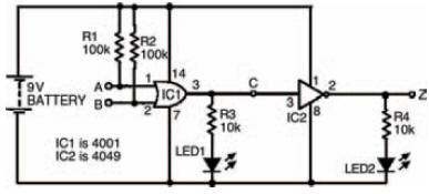
Figure 10.33 A simple circuit to create one type of gate (OR) from two other types (NOR and NOT)
A possible breadboard layout is shown in Figure 10.34, while an incomplete truth table is shown in Figure 10.35. Note that, as there are two stages to the circuit — that is, two separate logic gates — we can measure the middle section of the circuit by including another LED to more fully understand what’s going on inside the whole thing. Because of this, of course, the truth table needs to have an extra column to allow us to record the actions of the circuit as we carry out the experiment. Figure 10.36 shows a complete truth table for the circuit, which your results should mirror.
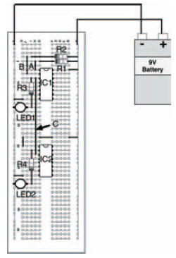
Figure 10.34 A breadboard layout for the experiment shown in Figure 10.33
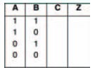
Figure 10.35 A truth table for you to record the results of your experiment
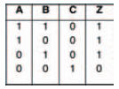
Figure 10.36 A completed truth table for the experiment of Figure 10.33
If we compare the truth tables (in either Figure 10.35 or Figure 10.36) with the truth table in Figure 10.14 we should see that the outputs are the same for the same inputs. (OK, yes, the inputs and output are presented in a different order — but the results are identical.)
In other words, we have used an inverter along with a NOR gate (by merely inverting the output of the NOR gate) to create an OR gate.
For completeness, Figure 10.37 shows a three input device based on this circuit, together with its truth table.
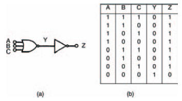
Figure 10.37 (a) using an inverter and a NOR gate to create an OR gate; (b) its truth table to prove this
OR and NOT gates combined
In the same vein as the last circuit, Figure 10.38 shows a circuit combining different types of logic gates — this time an OR gate whose inputs have been inverted by NOT gates. The outputs of both NOT gates (hence, also, the inputs of the OR gate) are measured with two LEDs, while the OR gate output is measured with the third LED.
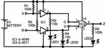
Figure 10.38 A circuit to investigate OR and NOT gates
Figure 10.39 shows a breadboard for the circuit for you to follow. Figure 10.40 shows an incomplete truth table for you to record your results of the experiment, while Figure 10.41 is a complete truth table, which — if everything goes as it should — your results will be identical to.
If you’ve already been thinking about this, you’ll no doubt already have been flicking back through this book’s pages to locate which truth table Figure 10.40 and 10.41 are identical to. If not, or if you simply haven’t found it, it’s the truth table in Figure 10.29 — which is that of a NAND gate.
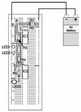
Figure 10.39 A possible breadboard layout for the circuit of Figure 10.38
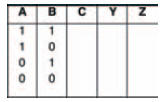
Figure 10.40 An incomplete truth table to record your experimental results
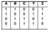
Figure 10.41 Complete truth table for the circuit of Figure 10.38
For the sake of completeness, Figure 10.42a shows a three input variant of this, and the accompanying truth table in Figure 10.42b shows the various logic levels in the circuit.
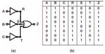
Figure 10.42 (a) a NAND gate, made from OR and NOT gates; (b) its truth table, to prove this
<< Simple, eh?