Logically speaking
In the electronic sense, digital signifies that a device has fixed states. Its input is either on or off, its output is also either on or off. As such there are only really two states, which incidentally gives rise to another term that is often used to describe such electronic circuits — binary digital. Also, it’s common to know the states by more simple names, such as on and off, or sometimes logic 0 and logic 1.
Hint:
States in an electronic digital circuit are generally indicated by different voltages, with a particular voltage implying one state, and another voltage implying the other state. The actual voltages are irrelevant, as long as it’s known which voltage implies which state, although by convention typical voltages might be 0 V when the state is off or logic 0, and 5 V when the state is on or logic 1. As long as there is a defined voltage for a defined state, it doesn’t matter. Further, and as a general rule, just the numbers 0 and 1 can be used to distinguish between the two logic states — whatever the voltages used.
In terms of electronic logic, the circuit of Figure 10.1 is quite simple in operation, and we can work out what it does by considering the transistor’s operation. We know from the experiment on page 174 that the presence of a small base current initiates a large collector current through the transistor. We can use this knowledge to calculate what happens in the circuit of Figure 10.1.
If the input at point A is logic 0 (we shall assume that logic 0 is represented by the voltage 0 V, and that logic 1 is represented by the voltage 10 V) then no base current flows, so no collector current flows — the transistor is switched off. This lack of collector current makes the transistor the equivalent of an extremely high resistance. An equivalent circuit representing this condition is shown in Figure 10.2, where the transistor resistance Rtr is 20 M (a typical value for a transistor in the off mode).
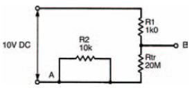
Figure 10.2 Equivalent diagram of a single transistor switch, with the transistor base (point A in Figure 10.1) connected to logic 0
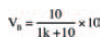
Resistors Rtr and R1 effectively form a voltage divider, the output voltage of which follows the formula:

which is close enough to being 10 V (that is logic 1) to make no difference.
The effect is that output B is connected to logic 1 — in other words, the output at point B is the opposite of that at point A.
If we now consider the transistor with a base current (that is, we connect point A to logic 1, at 10 V), the transistor turns on and passes a large collector current, with the effect that it become a low resistance. The equivalent circuit is shown in Figure 10.3.
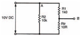
Figure 10.3 Equivalent diagram of a single transistor switch, with point A connected to logic 1
The output voltage at point B is now:
which is as close to 0 V (logic 0) as we’ll ever get.
So in this circuit the transistor output state is always the opposite of the input state. Put another way, whatever the input state, the output is always the inverse.
We call this simple digital circuit — you guessed it — an inverter.
<< Digital integrated circuits I