Reverse bias
From the curve you can see that there are two distinct parts which occur when a diode is reverse biased. First, at quite low reverse voltages, from about –0.V1 to the breakdown voltage there is a more or less constant but small reverse current. The actual value of this reverse current (known as the saturation reverse current, or just the saturation current) depends on the individual diode, but is generally in the order of microamps.
The second distinct part of the reverse biased characteristic occurs when the reverse voltage is above the breakdown voltage. The reverse current increases sharply with only comparatively small increases in reverse voltage. The reason for this is because of electronics breakdown of the diode when electrons gain so much energy due to the voltage that they push into one another just like rocks and boulders rolling down a steep mountainside push into other rocks and boulders which, in turn, start to roll down the mountainside pushing into more rocks and boulders, forming an avalanche. This analogy turns out to be an apt one, and in fact the electronic diode breakdown voltage is sometimes referred to as avalanche breakdown and the breakdown voltage is sometimes called the avalanche voltage. Similarly the sharp knee in the curve at the breakdown voltage is often called the avalanche point.
In most ordinary diodes the breakdown voltage is quite high (in the 1N4001 it is well over –50 V), so this is one reason why you couldn’t plot the whole characteristic curve, including reverse biased conditions, in the same experiment — ourbattery voltage of 9 V simply isn’t high enough to cause breakdown.
Some special diodes, on the other hand, are purposefully manufactured to have a low breakdown voltage, and you can use one of them to study and plot your own complete diode characteristic. Such diodes are named after the American scientist, Zener, who was one of the first people to study electronic breakdown. The zener diode you are going to use is rated at 3V0 which of course means that its breakdown occurs at 3 V which is below the battery voltage and is therefore plottable in the same sort of experiment as the last one. The symbol for a zener diode, incidentally, is shown in Figure 6.15.

Figure 6.15 The circuit symbol for a zener diode
Hint:
The way to remember the zener diode circuit symbol is to note that the bent line representing its cathode corresponds to the electronics breakdown.
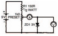
Figure 6.16 A circuit with the zener diode forward biased
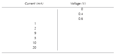
Table 6.5 Show the results of your experiment
Procedure is more or less the same as before. The circuit is shown in Figure 6.16 where the zener diode is shown forward biased. Complete Table 6.5 with the circuit as shown, then turn the zener diode round as shown in the circuit of Figure 6.17 (this is the way zener diodes are normally used) so that it is reverse biased, then perform the experiment again completing Table 6.6 as you go along. Although all the results will in theory be negative, you don’t need to turn the meter round or anything — the diode has been turned around remember, and so is already reverse biased.
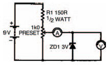
Figure 6.17 The circuit, with the zener diode reverse biased
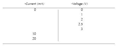
Table 6.6 To show the results of your further experiments
Next, plot your complete characteristic on the graph of Figure 6.18. My results and characteristics are in Table 6.7 and 6.8, and Figure 6.19. Yours should be similar.
From the zener diode characteristic you will see that it acts like any ordinary diode. When forward biased it has an exponential curve with a transition voltage of about 0V7 for the current range observed. When reverse biased, on the other hand, you can see the breakdown voltage of about –3 V which occurs when the reverse current appears to be zero, but in fact, a small saturation current does exist — it was simply too small to measure on the meter.
Figure 6.18 Plot your results from the zener diode experiment on this graph. Also use Table 6.6 shown on previous page
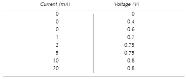
Table 6.7 The results of my experiments
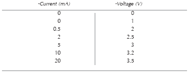
Table 6.8 More results from my experiments
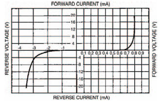
Figure 6.19 My results from the zener diode experiment are given in this graph and in Tables 6.7 and 6.8
Voila — a complete diode characteristic curve.
Finally, it stands to reason that any diode must have maximum ratings above which the heat generated by the voltage and current is too much for the diode to withstand. Under such circumstances the diode body may melt (if it is a glass diode such as the OA47), or, more likely, it will crack and fall apart. To make sure their diodes don’t encounter such rough treatment manufacturers supply maximum ratings which should not be exceeded. Typical maximum ratings of the two ordinary diodes we have looked at; the 1N4001 and the 0A47 are listed in Table 6.9.
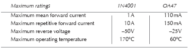
Table 6.9 Typical maximum ratings of the two diodes we have been looking at
Next chapter we shall be considering diodes again, and how we can use them, practically, in circuits; what their main uses are, and how to choose the best one for any specific purpose.
<< Tricky