Shutting the ’stable gate
All the digital electronic circuits we’ve looked at so far function more-or-less instantly. If certain inputs are present, a circuit will produce an output which is defined by the Boolean statement for the circuit — it doesn’t matter how complex the circuit is, a combination of inputs will produce a certain output.
For this reason, such circuits are known as combinational. While they may be used in quite complex digital circuits they are really no more than electronic switches — the output of which depends on the correct combination of inputs.
Put another way, they display no intelligence of any kind, simply doing what is demanded of them — instantly.
One of the first aspects of intelligence — whether in the animal world (including humans) or in the electronics world — is memory (that is, the ability to decide a course of action dependent not only on applied inputs but also on a knowledge of what has previously taken place).
Digital circuits can easily be made that remember logic states. We say they can store binary information. The family of devices that do that in digital electronics are known as bistable circuits (called this, because they remain stable in either of two states), sometimes also known as latches. It’s this ability to remain stable in either of the two binary states that allows them to form the basis of digital memory.
SR-type NOR bistable
The simplest bistable or latch is the SR-type (sometimes called RS-type) bistable, the operation of which acts like two gates connected together as in Figure 11.3. The circuit is constructed so that the two gates are cross-coupled — the output of the first is connected to the input of the second, and the output of the second is connected to the input of the first.
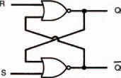
Figure 11.3 An SR-type bistable circuit, comprising two cross-coupled NOR gates
There are two inputs to the circuit, and also two outputs. The inputs are labelled S and R (hence, the reason why the circuits are called SR-type…), which stand for ‘Set’ and ‘Reset’. Now, it so happens that one output is, in most instances, the inverse of the other, so for convenience one output (by convention) is labelled Q and the other output (also by convention) is labelled (called bar-Q), to show this.
Both inputs to the SR-type NOR gate bistable should normally be at logic 0. As one input (either S or R) changes to logic 1, the output of that gate goes to logic 0. As the gates are crosscoupled, this is fed back to the second input of the other gate, which makes the output of the other gate go to logic 1. This, in turn, is fed back to the second input of the first gate, forcing its output to remain at logic 0 — even (and this is the important point) after the original input is removed. This is an important point!
Applying another logic 1 input to the first gate has no further effect on the circuit — it remains stable, or latched, in this state.
On the other hand, a logic 1 input applied to the other gate’s input causes the same set of circumstances to occur but in the other direction, causing the circuit to become stable, or latch, in the other way.
This sort of switching backwards and forwards in two alternate but stable states accounts for yet another term that is often applied to bistable circuits — they are commonly called ‘flip-flops’.
The SR-type NOR bistable operation can be summarised in a truth table, in a similar way that non-bistable or combinational logic gates can be summarised. However, because we are trying to tabulate inputs and outputs that change with time, then strictly speaking we should call this a ‘function table’, and such a function table for the SR-type NOR bistable is shown in Figure 11.4.
Account has been taken in the function table for changing from one logic state to the other, by the symbol , which indicates that the input state changes from a logic 0 to logic 1. Also, we no longer write the logic states as 1 and 0, but H (meaning high) and L (meaning low).
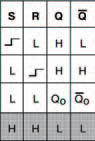
Figure 11.4 The function table of the SR-type NOR bistable circuit shown in Figure 11.3
The outputs indicate what happens as the input states change on these occasions. You can see that if input S goes high (that is, from 0 to 1) while input R is low, then the output Q will be high. If, however, input S then returns low, the output will be Q0 — which simply means that it remains at what it was. If input R then goes high while S remains low, the output changes to low and remains in that state even if R goes low again.
The last line of the function table is shaded to indicate that this condition is best avoided — simply because both outputs are the same. Designers of digital circuits would normally take steps to ensure that this condition did not occur in their logic circuits because confusion in the form of uncertain outcomes can obviously arise.
In other words (and, yes, I know that it was an awful lot of words), we have constructed a form of electronic memory, one of the outputs of which can be set to a high logic state by application of a positive-going pulse to one of its inputs. It’s a small, but, very significant advance — changing combinational logic gates into bistable circuits that can be used together to create sequences of logic level variations. In effect, what we have now done is to cross over from combinational logic circuits to a new type of logic circuits known as sequential logic circuits, with this simple but highly significant and very important addition of memory. Whatever we want to call them: bistables; latches; or flip-flops, they are sequential, and they can be used to create even more complex logic circuits.
SR-type NAND bistable
In Figure 11.3 the gates are both NOR gates, but they can be just as simply NAND gates, as shown in Figure 11.4. This gives us an SR-type bistable made from NAND gates. Easy enough — but there are some important considerations.
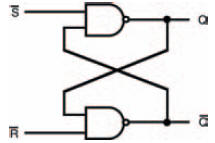
Figure 11.5 An SR-type bistable circuit comprising two cross-coupled NAND gates — note the inverted inputs when compared with Figure 11.3
The most important consideration is that both inputs of the SR-type NAND bistable should normally be at logic 1 — this is in direct contrast with the SR-type NOR bistable, where the inputs needed to be normally at logic 0. Because of this, the inputs are considered to be inverted in the circuit, shown as such in Figure 11.5.
With both inputs of the circuit of Figure 11.5 at logic 1, the circuit is stable, with both NAND gate outputs at logic 0. When one input goes to logic 1, the output of that NAND gate goes to logic 1. This is applied to the other NAND gate’s second input, so the output of the second NAND gate will go to logic 0. This output is in turn fed to the first NAND gate’s second input and thus its output is forced to remain at logic 1.
Applying a further logic 0 to the first NAND gate has no further effect on the circuit — it remains stable. However, when a logic 0 is applied to the second NAND gate’s input causes the same reaction in the other direction. So the circuit has two stable states, hence is a bistable.
Figure 11.6 shows the function table for this SR-type NAND bistable.
Just as in the SR-type NOR bistable, there is a possibility that both outputs can be forced to be the same level which produces an indeterminate outcome. In the SR-type NAND bistable, this is when both inputs are at logic 0. So, circuit designers must ensure this situation does not occur in their logic circuits.
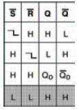
Figure 11.6 A function table for an SR-type NAND bistable circuit, such as that in Figure 11.5
While these simple gate circuits are really all that’s required to build bistables in theory, practical concerns require that something is added to them before they work properly and as expected. The problem is that the very act of applying changing logic levels to its inputs suffers from the mechanical limitations of the connecting method. Any mechanical switch (even one you might use in your home to turn on the lights) has ‘contact bounce’ — a phenomenon where the contacts in a switch flex while the switchover takes place, causing them to make and break the connection several times before they settle down.
Now, in the home, this is unnoticeable, because it happens so quickly you couldn’t see the light flickering due to it, even if the light itself could react that quickly. But digital circuits are quick enough to notice contact bounce, and as each bounce is counted as a pulse the circuit could have reacted many, many times to just one flick of the switch. While we were merely changing input states and watching output states of combinational logic circuits in the last chapter, this really didn’t matter. All we were wanting was a fixed output for a set of fixed inputs. In sequential circuits like bistables — and the other sequential circuits we’ll be looking at in this chapter, as well as others — contact bounce is a real problem, as we are wanting a sequence of inputs. The wrong sequence — given by contact bounces — will give us the wrong results. Simple as that!
The likes of simple bistables like the SR-type NAND bistable give us an ideal and effective solution to the problems created by contact bounce. We’ve just discussed how once one of the NAND gates in the circuit is switched by application of one logic 0 pulse at either it’s S or R input, it then doesn’t matter if any further pulses are applied to the input. So, a switch that provides the pulse could make as many contact bounces as it likes, the circuit will not be affected further.
Figure 11.7 shows the simple addition of a switch and two resistors to the SR-type NAND bistable, to give a circuit that can be used in other circuits to provide specific logic pulses that have absolutely no contact bounce.
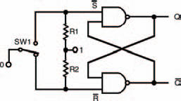
Figure 11.7 Simple circuit to prevent contact bounce
Switch SW1 in the circuit of Figure 11.7 is a simple single-pole, double-throw (SPDT) switch, and should have break-beforemake contacts (in other words, when switching from one connection to the other, its switch contacts will disconnect from one connection before it connects to the other — so there is a point in the switch motion when all three contacts are disconnected from each other). The switch can be either a push-button switch, or a conventional flick-type switch.
Operation is fairly simple. At rest, one of the NAND gate inputs connects through the switch to logic 0, while the other NAND gate’s input is connected through a resistor to logic 1. As the switch is switched, the second NAND gate’s input is connected to logic 0 though the switch, and the circuit operates as previously described like a standard SR-type NAND bistable. It doesn’t matter whether there is contact bounce or not at this time, as repeated pulses do not affect the bistable.
When the switch is operated again, so the first NAND gate’s input is connected to logic 0 and the bistable jumps to its other stable state. Again, contact bounce will make no difference to it.
One or both of the outputs of the simple de-bouncing circuit can be applied to the inputs of following circuitry, safe in the knowledge that contact bounce will have no effect. The requirement for no contact bounce is true for any sequential circuit, actually. So this very simple solution can be used not just in the simple circuits we see here in this chapter, but for all sequential circuits. Whenever a sequential logic circuit requires a manually pulsed input, this circuit can be used.
<< IC series